Silicon wafer crack detection module
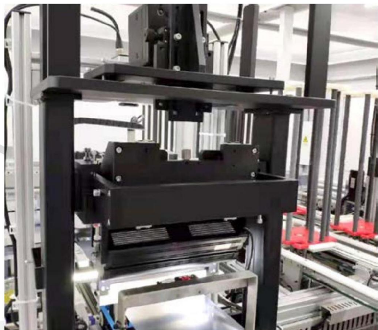
Use OfEquipment:
The principle of infrared imaging is used to detect hidden cracks, perforations, missing angles, foreign bodies and other defects when the silicon wafer is put on, and the defective products are automatically removed to improve the product pass rate.
Product Features:
Optimize the light source index: adopt a customized band LED light source to improve the service life of the light source, improve the imaging effect, and output more stable images;Upgrade processing algorithm: The introduction of a deep learning framework improves the detection effect of fine cracks and linear and horizontal effects, and achieves better stability.